Tech Tips
Conductive Prints for Wearable Electronics in a Manufacturing Plant
Abstract
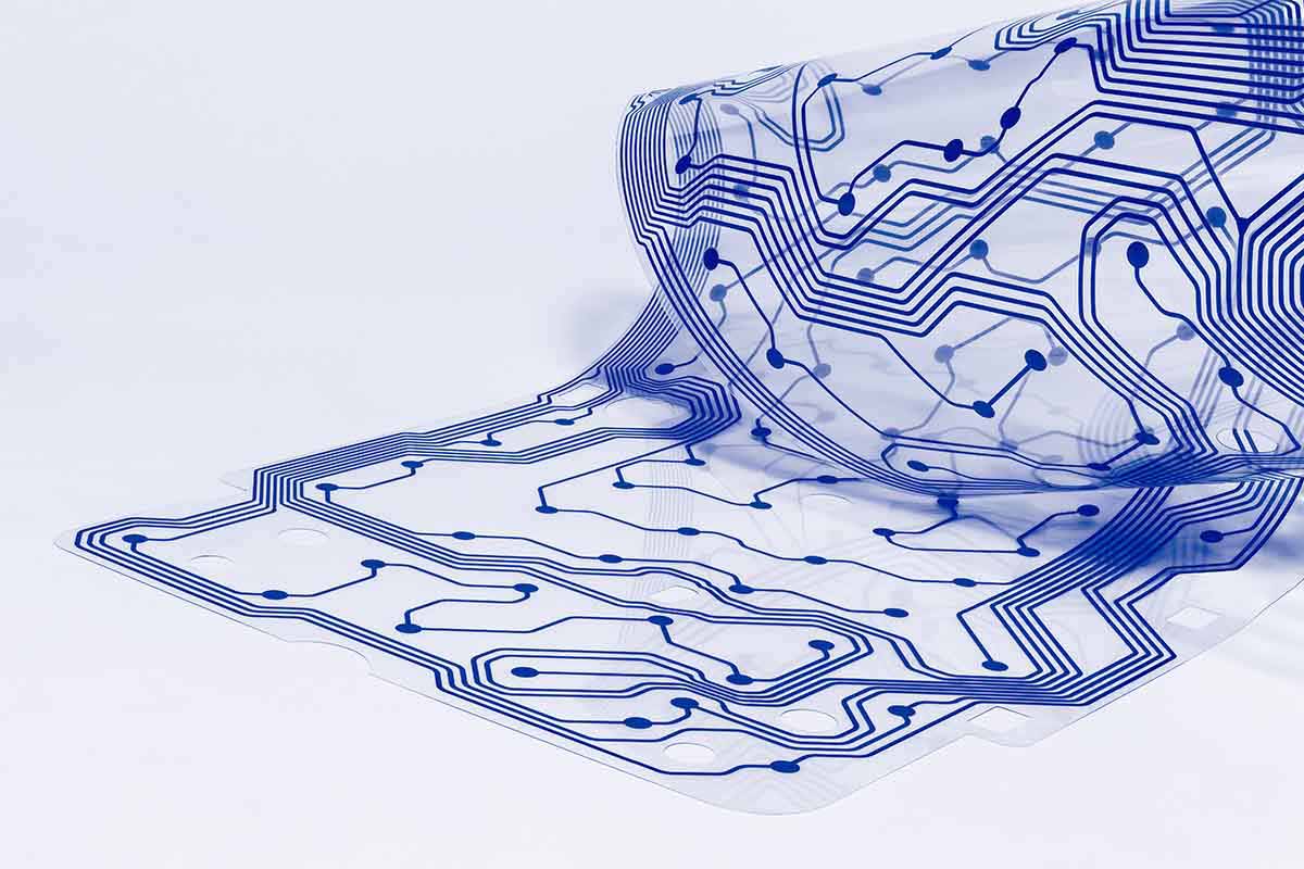
Wearable electronics, as a value-added extension of Flexible Electronics, requires the right combination of a flexible substrate, a wetting ink, and high-fidelity roll-to-roll (R2R) print for the target circuit design. The resulting circuit should be able to maintain its electronic integrity when conforming to the body contours of the wearer and many cycles of bending and twisting during use. To that end, any post-print modification such as embossing or perforation may be applied without compromising performance. Flexcon Global, as a full-service company, is well positioned to meet these requirements seamlessly from design to production.
Introduction
Flexible electronics, the technology of laying electronic devices on a flexible polymer surface rather than a rigid solid board, offers the advantages of size, shape, light weight, and portability. This can be promoted to wearable electronics when the electronic device or sensor is integrated into clothing, jewelry, or other accessories. Wearable electronics would often need functional elements such as a power source, sensor transducer, and low impedance bus bars for an active device such as a transistor, or at least some precision prints for a passive device such as an antenna. In either case, the print should be such that the integrity of the circuit remains intact despite the strains sustained in its operations, a natural corollary to the use of a wearable electronics gadget. The design for wearable electronics involves selections of the right substrates, appropriate inks, and suitable coating methods and after the print, any unique process step that would enhance the device flexibility and performance can be added in.
Substrates:
For the substrate to be suitable for wearable electronics, it must be flexible and mechanically strong to survive all the bends, twists, and motions of the wearer besides being breathable for comfort. The printed circuits need to stay intact without sustaining any strain-induced damage and, desirably, be as imperceptible as possible. Significant challenges arise when designing strain tolerant electronic devices that can be conformally mounted on non-uniform or non-planar surfaces. Thus, any substrate for this purpose should have the right tensile properties; i.e., low Young’s modulus (Y) and high tensile strength. The human skin epidermis layer has a Young’s modulus of 50-100 kPa. Compared to it, many of the commonly used polymer substrates for wearable electronics are stiff but acceptable such as polyethylene naphthalate (PEN; Y = 4 GPa), polyethylene terpthalate (PET; Y = 2.5 GPa), polyimide (PI; Y = 2.3 GPa), thermoplastic urethane (TPU; Y = 3.6-88.8 MPa), polydimethylsiloxane (PDMS; Y = 0.5-3 MPa). [1-8]
To ensure good adhesion of the ink to the substrate, the surface energy of the substrate should adequately match that of the ink. For example, most water-based inks would require low surface energy substrates (less than 36 dynes/cm); e.g., polyolefins, but organic solvent-based inks need high surface energies. The surface energy of a substrate can be manipulated by subjecting the surface to corona treatment; i.e., exposing the surface to a low temperature corona discharge of air plasma which results in an increase in the surface energy. The effect of the corona treatment is short lived and, therefore, the printing/coating of the substrate should follow the treatment without a huge gap of time. In most cases, it is recommended that the gap not exceed 28 days.9
Conductive Silver Inks:
There has been much progress in the development of conductive inks for use as bus bars; but the most ubiquitous ink for flexible electronics is silver ink, with the flake-based silver ink (10−15 mΩ/□/mil) being the most used. The regular flake-based commercial silver ink, while it has an established high performance in plastic-based flexible electronics, still has the limitations of not meeting the requirements of highly fine line circuits. Besides, it undergoes fractures of the print because of cycles of strains in the use of wearable electronics. Nanoparticles-based silver inks have been found to offer comparable good conductivity (~15 mΩ/□/mil) while enabling more compact circuitry and easier laying of finer lines compared to the flakes-based silver inks. Yet, there are reports of molecular silver ink which essentially is a silver organometallic that would decompose to give metallic silver during the curing process, thus it avoids the issues of a particles-based inks such as proneness to fracture and inter-grain boundaries that can raise the resistances.
Thus, depending on the fineness of the circuitry and electrical property requirement, one or the other ink, or a formulation from the combination thereof, can be of optimal use.
Printing Methods:
For conductive prints, some of the popular printing methods are gravure, aerosol jet, inkjet, and screen printing. Among these, gravure and screen printing are R2R industry friendly processes in terms of scale, though screen printing is more economical as rotary screens are much cheaper than gravure drums. In screen printing, the resolution of the print is governed by the mesh size of the screen, particle sizes of a particles-based ink, and the viscosity (typically 4000-12000 cP). The rotary screen process involves the use of a cylindrical screen, which is typically made of nickel or stainless steel mesh. The screen is coated with a photosensitive emulsion which is then exposed to a film positive that contains the image or design (circuit pattern) to be printed. The exposed emulsion is then washed away, leaving a stencil of the image on the screen. A high-fidelity reproduction of the circuit pattern is, thus, possible for an industry quantity of web length of the suitable flexible substrate. Depending on the ink composition and the print thickness, the speed of printing can have a wide range from 1-2 ft to 400-500 ft per minute of the web.
Post Print Value Addition:
A flexible circuit print is supposed to survive stretch due to body contours as well as bending and twisting for thousands of cycles to even merit the designation of wearable electronics. A conductive print, despite the availability of fine particles size and no-grain inks, still suffers from mechanical fatigue and cracks during use. A value addition proposition for obtaining even greater flexibility and preventing cracks is to perforate the device print area by via holes of a few microns in diameter. The via holes provide an environment where the crack sizes on the substrate decrease overall by concentrating the stress at the hole site rather than propagating long range. For devices that are DC voltage based or AC voltage based with low frequencies, there is no practical effect in their performances. It has been found that for thin film transistors, the percentage of resistance rises due to bending decreases if there are more via holes.10 Thus, particularly for bus bar prints, a 10-25% area of the printed circuits micrometer size holes could be recommended for the value addition.
Flexcon on Conductive Print:
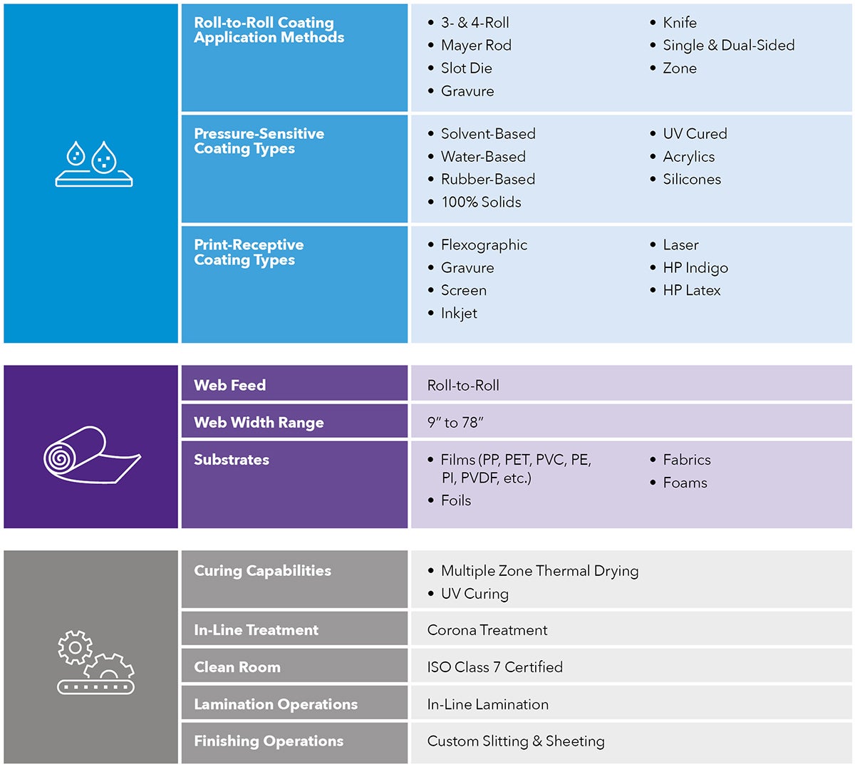
Flexcon, a global manufacturer with its headquarters in Massachusetts, USA and many branches worldwide, has considerable expertise and capabilities on R2R web printing. For conductive prints, a R2R screen printer is dedicated with the option of any environmental control, if needed.
In addition, it has many other post-print processes such as multilayer lamination, slitting, brushing, micro-embossing, perforation, etc. which can add value enhancement to a conductive print (Fig. 1). For example, micro-embossing and micro-perforation can structure the surface of a printed web and may improve flexibility as well as aid in the addition of another functional layer.
In Flexcon’s Business, Technology and Discovery (BTD) group, the approach to a successful conductive print for wearable electronics includes studying the adhesion of the ink on a wearable substrate involving a print head (e.g., R2R screen printer) on the actual plant floor after some small scale rapid prototyping. The print widths and lengths are highly customizable to suit the scale of test, often with the help of an appropriate displacement block in an ink pan in the event of a small supply of ink (say, 0.5 gallon). Further, all the post-print processing is carried out on the same scale. This practice makes it fairly conclusive that the performance of a functional print at a true manufacturing scale will replicate well.
References:
- D. H. Kim et al., “Epidermal electronics,” Science 333, 838 (2011).
- M. Kaltenbrunner et al., “An ultra-lightweight design for imperceptible plastic electronics,” Nature 499, 458 (2013).
- J. W. Jeong et al., “Wireless optofluidic systems for programmable in vivo pharmacology and optogenetics,” Cell 162, 662 (2015).
- R. C. Webb et al., “Ultrathin conformal devices for precise and continuous thermal characterization of human skin,” Nat. Mater. 12, 938 (2013).
- V. Kanyanta and A. Ivankovic, “Mechanical characterisation of polyurethane elastomer for biomedical applications,” J. Mech. Behav. Biomed. Mater. 3, 51 (2010).
- J. W. Jeong et al., “Materials and optimized designs for human-machine interfaces via epidermal electronics,” Adv. Mater. 25, 6839 (2013).
- K. I. Jang et al., “Rugged and breathable forms of stretchable electronics with adherent composite substrates for transcutaneous monitoring,” Nat. Commun. 5, 4779 (2014).
- D. Qi et al., “Highly stretchable, compliant, polymeric microelectrode arrays for in vivo electrophysiological interfacing,” Adv. Mater. 29, 1702800 (2017).
- https://tantec.com/basics-of-corona-treatment/
- Gwang Jun Lee et al., "Stress Release Effect of Micro-hole Arrays for Flexible Electrodes and Thin Film Transistors", ACS Appl. Mater. Inter. 12, 19226 (2020)