Live Webinar: Discover the benefits of hydrogel-free bio-sensing
Solving the limitations of hydrogels in wearable and diagnostic technology
Thursday, May 16
11:00 AM - 11:30 AM EDT

Tech Tips
From Outer Space to the Exam Room
Developing Flexible Electronics for Comfort, Efficacy for Remote Medical Patient Monitoring
Used with permission of Converting Quarterly. Copyright 2021 Q4, Peterson Publications, Inc. (Topeka, KS)
Many technologies available to us today, such as drones and self-driving cars, started life at NASA. The same is true for certain healthcare technologies, including remote medical monitoring. First developed as a means to monitor the vital signs of astronauts in space, remote medical monitoring is fast becoming mainstream, especially because the pandemic made telehealth the rule rather than the exception. Remote sensing devices enable healthcare providers to monitor and diagnose conditions related to a variety of systems, such as cardiac function and glucose levels. In fact, the global market for remote patient monitoring (RPM) systems is expected to reach $1.7 billion by 2027. [i]
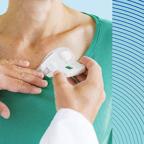
One challenge with remote monitoring, however, is patient compliance. For the medical provider to obtain reliable data, the patient must wear the device correctly and consistently. Historically, such devices have been uncomfortable and have hindered regular activities due to bulky wires and electrodes, leading to unreliable patient compliance. Wearable devices that are adhered directly to the skin have been a great improvement; however, rigid devices can still be uncomfortable.
Enter Flexible Electronics
Thanks to flexible electronics (FE), medical sensing patches are paving the way for better patient compliance because they can do the job of rigid monitoring devices while allowing for a nearly set-it-and-forget-it scenario. Made from a combination of flexible films, conductive inks and bio-compatible adhesives, they can move and stretch with the body. Once applied, the wearer can simply go about their business while the device does its job. The FE embedded within the device conduct physiological signals from the body to be stored in a chip within the patch, and while the chip is rigid, it requires a very small footprint, with the majority of the device being comprised of flexible, skin-friendly materials. Such devices are becoming very popular with both patients and providers, and the market for FE in the healthcare space is expected to exceed $8.3 billion by 2030. [ii]
The creation of medical sensing patches involves multiple components, which generally include:
- a chip to collect and store information;
- a conductive ink to pass physiological signals from the body to the chip;
- dielectrics to insulate the conductive layer(s) as well as the chip;
- an antenna (which may be comprised of the conductive ink) to relay data to a mobile device such as a smartphone or to a physical receiver;
- a battery to power the device;
- adhesive layers to hold it all together;
- an elastomeric material coated with a skin contact adhesive to adhere the device to the body; and
- an environmental layer to protect all components from external exposures, such as abrasion, water and humidity, alcohol, personal care products, or anything else that might come in contact with a patient’s skin.
The number and order of the layers will vary depending on the specific device.
For converters to be successful in running jobs comprised of all these functional components, knowing exactly what their equipment can and cannot do is vital. Converters can provide valuable input to device design based on their equipment capabilities and processing expertise which can help determine ink and adhesive chemistries, substrate selection for both conductive and dielectric layers as well as adherence to the body, and how the device will receive and send signals, such as through a Bluetooth or plug-in connection.
FE Basics
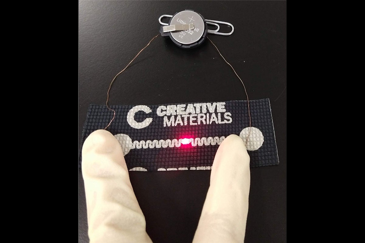
The key components that make a flexible electronic patch possible are conductive inks which relay signals to a chip, the dielectrics that will surround them to maintain separation of the conductive pathways or traces, and the adhesives that will hold everything together as well as adhere it to the body.
Conductive Layers
Conductive materials allow the flow of a charge in one or more directions. Metals such as gold, silver and copper are widely used conductors. In a FE device, the conductors are not solid wires, but rather inks comprised of fragments of the conductive material along with a binder that holds them together. This fragmentation is what enables their flexibility. The most common conductive inks are made from silver, gold, copper or carbon. Other possibilities include exotic metals or inherently conductive polymers; however, their use is rare and limited to niche applications.
The polymer used to bind the conductive fragments together will be chosen based on the intended purpose. Binders used in the ink must be compatible with the substrate on which they will be printed. Like printing graphics on any film substrate, the ink must be able to adhere to remain functional. Certain films are more porous and, therefore, receive inks better. In graphics production, for example, vinyls are inherently printable whereas polyesters require a topcoat for inks to adhere. FE applications are no different, and it is possible to use a binder that “likes” the film to which it will be applied. Polyimide is quite often the binder system of choice because polyimide is frequently the dielectric that will be used due to its durability and flexibility.
Ink choice will depend on factors such as conductivity (Table 1), oxidation rate, printability and stability. From the viable choices of silver, gold and copper, silver is often preferred because it enjoys excellent printability, and any mild surface oxidation to silver oxide does not impair its stability and conductivity value. However, there is a legitimate apprehension that silver may initiate its anti-microbial effect and thus destroy the efficacy of biological reagents. In comparison, gold will not oxidize or kill reagents; however, the higher associated cost often precludes its use. Copper is another viable option, but for short-term applications only due to its shorter-term oxidation rate.
Dielectric Layer(s)
A dielectric is an insulating or capacitive material and has high resistance to electron flow. It covers the circuits created by the conductive inks in the X and Y directions and, if capacitive, can allow minute traces in the Z direction from the skin to the chip while isolating them from each other. Its purpose in a FE device is to prevent circuits from becoming compromised or broken, prevent shorting, and add mechanical durability. Any failure of the dielectric will result in unwanted electrical coupling between the traces and lead to cross-talk, inaccurate data or failed transmission altogether. Cross-talk is interference caused by electromagnetic signals that will affect another electronic signal. An analogy would be a noise or squealing while there is communication between devices, such as a microphone and speaker feeding back. The dielectric constant (DK) of the material, which is a measure of its ability to store electrical energy, will determine how tight the spacing of the conductive pathways can be. The dissipation factor (DR), which is a measure of the rate at which the material loses energy, typically in the form of heat, will also impact spacing. A good insulator will have a high DK and a low DF, allowing for the circuitry to be smaller and, therefore, the device to be smaller.[iv]
Some of the most common dielectric materials are glass, Teflon, polyethylene, polyimide, polypropylene, polystyrene, and titanium dioxide, but there are many more. Selection of the dielectric will depend on the flexibility required for the application as well as anticipated exposures.
The most popular dielectric by far is polyimide. Polyethylenes and polypropylenes may seem like good choices because they are inexpensive, have low moisture uptake and are flexible; however, they are limited in terms of temperature resistance, and they have very low surface energy, making them difficult to bond to. Polyimide offers better bonding and, while it is more expensive and more rigid than PE or PP, a secure bond of ink to substrate is essential for conductivity. Furthermore, this more costly, high-performing material can be used in a vary small area of the device specifically for the electronics, with cheaper components being utilized for portions that don’t need to carry any current.
Adhesives
Commonly used adhesives in FE devices are polyamides (nylons), polyesters, polyurethanes, butyl rubbers, and many more. Adhesive choice will depend on the functionality required – flexibility, application clarity, and method of application. A visco-elastic adhesive is always under flow, meaning that it remains flexible, which can be ideal for a wearable diagnostic patch. Other adhesive types include thermal set adhesives, which harden once they are crosslinked and cured, and thermoplastic adhesives, which flow when they are warm and bond when cold. If reheated, however, they can reflow. It’s possible for multiple adhesive types to be needed within the same device. For example, a thermal set adhesive may be required to seal around the chip to prevent moisture from penetrating, while a thermoplastic adhesive may be desired to surround the conductive pathways because it will remain flexible as the patch becomes distorted with body movement. This functionality will help maintain conductivity of the ink layers. With a wearable device application, a skin-compatible adhesive approved under ISO 10993 will also be required for adhering the device to the skin. Wear duration will impact adhesive choice. There are many options available, including silicones and low-peel acrylics for gentle release/short-term wear, as well as general purpose and higher strength acrylics for moderate to long-term anchorage.
Processing Considerations
Registration Tolerances
One of the goals in constructing a flexible diagnostic patch is for it to be as unobtrusive as possible. The smaller the circuitry can be printed, the smaller the device can be. In addition, circuitry that takes up less area will be flexed less, decreasing the possibility of damaged circuits with body movement over time. To accomplish this, feature sizes of printed electronics must be extremely small (as small as a 5-mil line space), so knowing the tolerances within which printing and cutting equipment can function in both alignment and dimension will be essential to ensuring an acceptable signal is achieved.
Curing/Drying
Air dry, IR, UV and photonic sintering are all cure methods that might be utilized. The goal, of course, is to generate the right amount of energy to cure the ink. There may be instances where the ink may require more heat to cure than other components can tolerate. Photonic sintering is a cure method by which energy in the form of a laser or pulsed light is directed at only the ink rather than the entire substrate. This enables the ink to reach the cure temperature much more quickly without compromising any temperature-sensitive materials or components in the rest of the construction. On the other hand, the less directed cure methods are still viable options and, in many cases, preferred due to lower cost and expediency. [vi]
Connection Method
The device may be connected to the receiver physically or wirelessly. For a physical connection, such as an external power source or reader, a connector may be required. Because elastomeric materials typically used to adhere a medical sensing patch to the body are flexible, a clincher connection may be appropriate. A clincher style connector compresses metal contacts into the substrate without need for insertion or soldering. However, quite often even a flexible patch would utilize spring loaded contacts that a receiver would be plugged into, either during use or following use to capture data. In such cases, a zero-insertion force (ZIF) connection may be utilized. This may require the use of a protective layer of the contacts and a stiffener to allow for ease of plugging in. Designers may inquire as to multiple connecter options based on functionality or cost, so it’s important to know what is implementable from the converter’s standpoint and the associated costs.[vii]
Circuitry Design
Elongation of the base material will affect resistance of the printed circuits, and the circuit pattern design can impact performance of the device. Understanding how much the item might need to stretch is critical to ensuring the change in resistance won’t become so high as to interrupt the current. Typically, the change in resistance is minimal with a small amount of elongation but rises exponentially with greater elongation[viii]. A serpentine pattern is often used to mitigate the effects of the base material stretching, much like a coiled phone cord protects the wire inside from breaking when stretched.
Testing
A copious amount of testing is needed specific to performance criteria required for the application. This will include testing of each individual component on its own followed by testing of various components together as well as the final construction. The testing required for any particular device will be driven by identification of the critical success factors, such as a DK higher than X, moisture vapor transmission rate lower than Y, or bond strength higher than Z.
Beyond general component testing, examination of the electrical properties to ensure proper conductivity and function of the device is essential. This includes identification of the range in which the device, as a whole, must perform and confirmation that conductivity will persist so as to achieve desired outcomes.
Resistivity
Resistivity is a measure of resistance derived from the ratio of voltage to current which indicates how strongly a material resists an electrical current. Resistance of the conductive pathways will be impacted by certain factors such as elongation, and testing enables designers to understand those tolerances. As resistance rises, heat is produced. Too much heat leads to device failure.
Flexibility/Creasability
Finding the right recipe for a medical diagnostic patch or any FE device is a matter of balancing the efficacy of each component and its compatibility with the other components, along with the cost of each, and then determining the most appropriate processes. Starting with the highest-performing components that can work together, and then determining what processes and components are feasible from both a processing and cost perspective is a good method for bringing the right pieces together. If cost is prohibitive, then experimentation can happen with less expensive components and varying processes until the desired result is achieved. Finding that balance is the key, and collaboration among designers, component suppliers and converters will be the driving force that brings FE projects to fruition to address the needs of patients and providers alike.
Environmental Performance
Environmental testing will ensure that the device can withstand expected environmental exposures. Examples include QUV or Xenon Arc accelerated weather testing, moisture resistance if the device needs to be watertight, testing of oxygen transmission rate, and clarity/opacity testing if readings will need to be taken through the environmental layer or if an opaque aesthetic is desired.
Looking to the Future
Continual advancements in technologies through new materials and processes are being driven by consumer demand and, in the medical space, by provider demand as well. Inks with higher conductivity that can function at higher operating temperatures are in development as are more flexible inks for textiles and in-mold components. Furthermore, lower temperature and solderable inks are decreasing the barriers to manufacturing and enabling more efficient processes. This, in turn, will enable manufacturers to meet the increasing demand for smaller and more sophisticated devices in the medical space and beyond.
Balancing Act
Finding the right recipe for a medical diagnostic patch or any FE device is a matter of balancing the efficacy of each component and its compatibility with the other components, along with the cost of each, and then determining the most appropriate processes. Starting with the highest-performing components that can work together, and then determining what processes and components are feasible from both a processing and cost perspective is a good method for bringing the right pieces together. If cost is prohibitive, then experimentation can happen with less expensive components and varying processes until the desired result is achieved. Finding that balance is the key, and collaboration among designers, component suppliers and converters will be the driving force that brings FE projects to fruition to address the needs of patients and providers alike.
[i] S. Dolan The technology, devices, and benefits of remote patient monitoring in the healthcare industry (2021) https://www.businessinsider.com/remote-patient-monitoring-industry-explained
[ii] Cision Flexible Electronics Are the Future in Wearable Health Monitoring (2020) https://www.prnewswire.com/news-releases/flexible-electronics-are-the-future-in-wearable-health-monitoring-301049589.html
[iii] Li, Jiaxiang & Li, Yunping & Wang, Zhongchang & Bian, Huakang & Hou, Yuhang & Wang, Fenglin & Xu, Guofu & Liu, Bin & Liu, Yong. (2016). Ultrahigh Oxidation Resistance and High Electrical Conductivity in Copper-Silver Powder. Scientific Reports. 6. 39650. 10.1038/srep39650.
[vi]Britannica, The Editors of Encyclopaedia. "Dielectric constant". Encyclopedia Britannica, 28 May. 2020, https://www.britannica.com/science/dielectric-constant. Accessed 2 August 2021.
[v] Jongsu Lee, Jinwoo Seong, Janghoon Park, Sungsik Park, Dongjin Lee, Kee-Hyun Shin,
Register control algorithm for high resolution multilayer printing in the roll-to-roll process,
Mechanical Systems and Signal Processing, Volumes 60–61, 2015, Pages 706-714, ISSN 0888-3270, https://doi.org/10.1016/j.ymssp.2015.01.028. (https://www.sciencedirect.com/science/article/pii/S0888327015000394)
[vi] Roberson, D., Wicker, R. & MacDonald, E. Ohmic Curing of Printed Silver Conductive Traces. Journal of Elec Materi 41, 2553–2566 (2012). https://doi.org/10.1007/s11664-012-2140-4
[vii]Mitsui, R.; Sato, J.; Takahashi, S.; Nakajima, S.-i. Electrical Reliability of a Film-Type Connection during Bending. Electronics 2015, 4, 827-846. https://doi.org/10.3390/electronics4040827
[viii] Donald Christiansen; Charles K. Alexander; Ronald K. Jurgen. Standard Handbook of Electronic Engineering, Fifth Edition (McGRAW-HILL, 2005). https://www.accessengineeringlibrary.com/content/book/9780071384216
Authors:
Mike Merwin is the Manager, Business and Technology Discovery at Flexcon Company, Inc. (Spencer, MA). Mike has worked with polymeric coating for over 40 years and has served in a variety of roles in technical service and product development creating functional technologies for existing and emerging markets. He is a member of the Society of Plastic Engineers and the Department of Energy/Advanced Manufacturing Office, serving on the Industry Engagement Panel for the R2R Collaboration.
Aaron Elman is the Manager of Business Operations for Business and Technology Discovery at Flexcon Company, Inc. (Spencer, MA). He holds a degree in Chemistry from the University of Connecticut. Aaron has worked at Flexcon for over seven years. At Flexcon, he has worked in Research and Development specializing in polymeric substrates and web-based technologies. Additionally, he currently is within the Business and Technology Discovery Group developing and commercially scaling novel chemistries from prototype to full roll-to-roll production.
Jonathan Knotts is the Applications Engineering Manager at Creative Materials. Jonathan studied chemical engineering at the University of New Hampshire and also holds a degree in plastics engineering from University of Massachusetts Lowell. Jonathan has been developing materials and new technology at Creative Materials for more than 15 years. A leading expert in advanced material technology and performance composites, Jonathan is involved in development, implementation, and technical support. As the director of the research and development department, he is responsible for successful product placement in emerging technologies.
Lynn Rodman is a Subject Matter Expert, Advanced Materials at NeXolve Holding Company, LLC (Huntsville, AL). Lynn joined NeXolve in 2009 where he has worked as an analytical and polymer chemist with specialty in synthesis and characterization of high temperature polyimide materials. He holds a Ph.D. in Analytical and Polymer Chemistry from the University of Tennessee, Knoxville.